- 您现在的位置:买卖IC网 > Sheet目录2008 > MAX1394ETB+T (Maxim Integrated Products)IC ADC 8BIT 416KSPS 10-TDFN-EP
MAX1391/MAX1394
2
_______________________________________________________________________________________
1.5V to 3.6V, 416ksps, 1-Channel True-Differential/
2-Channel Single-Ended, 8-Bit, SAR ADCs
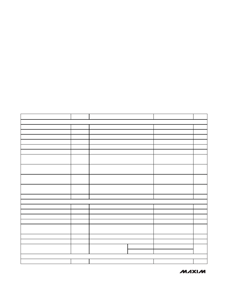
ABSOLUTE MAXIMUM RATINGS
ELECTRICAL CHARACTERISTICS
(VDD = +1.5V to +3.6V, VREF = VDD, CREF = 0.1F, fSCLK = 5MHz, TA = TMIN to TMAX, unless otherwise noted. Typical values are at
TA = +25°C.) (Note 1)
Stresses beyond those listed under “Absolute Maximum Ratings” may cause permanent damage to the device. These are stress ratings only, and functional
operation of the device at these or any other conditions beyond those indicated in the operational sections of the specifications is not implied. Exposure to
absolute maximum rating conditions for extended periods may affect device reliability.
VDD to GND ..............................................................-0.3V to +4V
SCLK, CS, OE, CH1/CH2, UNI/BIP,
DOUT to GND.........................................-0.3V to (VDD + 0.3V)
AIN+, AIN-, AIN1, AIN2, REF to GND ........-0.3V to (VDD + 0.3V)
Maximum Current into Any Pin .........................................±50mA
Continuous Power Dissipation (TA = +70°C)
10-Pin TDFN (derate 18.5mW/°C above +70°C) ....1481.5mW
Operating Temperature Ranges
MAX139_E_ _...................................................-40°C to +85°C
Junction Temperature ......................................................+150°C
Storage Temperature Range .............................-60°C to +150°C
Lead Temperature (soldering, 10s) .................................+300°C
PARAMETER
SYMBOL
CONDITIONS
MIN
TYP
MAX
UNITS
DC ACCURACY (Note 2)
Resolution
8
Bits
Integral Nonlinearity
INL
±0.2
LSB
Differential Nonlinearity
DNL
No missing code overtemperature
±0.2
LSB
Offset Error
±0.15
LSB
Gain Error
Offset nulled
±0.15
LSB
Total Unadjusted Error
TUE
±0.25
LSB
Offset-Error Temperature
Coefficient
±25
mLSB/°C
Gain-Error Temperature
Coefficient
±0.06
mLSB/°C
Channel-to-Channel Offset
Matching
MAX1394 only
±0.05
LSB
Channel-to-Channel Gain
Matching
MAX1394 only
±0.05
LSB
Input Common-Mode Rejection
CMR
VCM = 0 to VDD, MAX1391 only
±0.1
mV/V
DYNAMIC SPECIFICATIONS (Note 3)
Signal-to-Noise Plus Distortion
SINAD
49
dB
Signal-to-Noise Ratio
SNR
49
dB
Total Harmonic Distortion
THD
-65
dBc
Spurious-Free Dynamic Range
SFDR
-66
dBc
Intermodulation Distortion
IMD
fIN1 = 98kHz at -6.5dBFS,
fIN2 = 102kHz at -6.5dBFS
-73
dB
Channel-to-Channel Crosstalk
MAX1394 only
-70
dB
Full-Power Bandwidth
-3dB point
4
MHz
MAX1391
200
Full-Linear Bandwidth
SINAD > 48dB
MAX1394
150
kHz
CONVERSION RATE
Conversion Time
tCONV
9 clock cycles per conversion
1.8
s
发布紧急采购,3分钟左右您将得到回复。
相关PDF资料
MAX1395ETB+T
IC ADC 10BIT 357KSPS 10-TDFN
MAX1400CAI+
IC ADC 18BIT LP 28-SSOP
MAX1401CAI+
IC ADC 18BIT LP 28-SSOP
MAX1415AEWE+T
IC ADC 16BIT DELTA SIGMA 16-SOIC
MAX1421CCM+D
IC ADC 12BIT 40MSPS 48LQFP
MAX1426EAI+T
IC ADC 10BITS 10MSPS 28SSOP
MAX1434ECQ+D
IC ADC 10BIT 50MSPS 100-TQFP
MAX1444EHJ+T
IC ADC 10BIT 40MSPS 32-TQFP
相关代理商/技术参数
MAX1394ETB-T
功能描述:模数转换器 - ADC RoHS:否 制造商:Texas Instruments 通道数量:2 结构:Sigma-Delta 转换速率:125 SPs to 8 KSPs 分辨率:24 bit 输入类型:Differential 信噪比:107 dB 接口类型:SPI 工作电源电压:1.7 V to 3.6 V, 2.7 V to 5.25 V 最大工作温度:+ 85 C 安装风格:SMD/SMT 封装 / 箱体:VQFN-32
MAX1394MTB+T
功能描述:模数转换器 - ADC 8-Bit 2Ch 400ksps 3.6V Precision ADC RoHS:否 制造商:Texas Instruments 通道数量:2 结构:Sigma-Delta 转换速率:125 SPs to 8 KSPs 分辨率:24 bit 输入类型:Differential 信噪比:107 dB 接口类型:SPI 工作电源电压:1.7 V to 3.6 V, 2.7 V to 5.25 V 最大工作温度:+ 85 C 安装风格:SMD/SMT 封装 / 箱体:VQFN-32
MAX1394MTB-T
功能描述:模数转换器 - ADC RoHS:否 制造商:Texas Instruments 通道数量:2 结构:Sigma-Delta 转换速率:125 SPs to 8 KSPs 分辨率:24 bit 输入类型:Differential 信噪比:107 dB 接口类型:SPI 工作电源电压:1.7 V to 3.6 V, 2.7 V to 5.25 V 最大工作温度:+ 85 C 安装风格:SMD/SMT 封装 / 箱体:VQFN-32
MAX1395ETB
制造商:Maxim Integrated Products 功能描述:1.5V-3.6V357KSPS1-CHANNEL TRUE-DI - Rail/Tube
MAX1395ETB+
制造商:Maxim Integrated Products 功能描述:ADC SGL SAR 357KSPS 10-BIT SERL 10TDFN EP - Rail/Tube
MAX1395ETB+T
功能描述:模数转换器 - ADC 10-Bit 2Ch 357ksps 3.6V Precision ADC RoHS:否 制造商:Texas Instruments 通道数量:2 结构:Sigma-Delta 转换速率:125 SPs to 8 KSPs 分辨率:24 bit 输入类型:Differential 信噪比:107 dB 接口类型:SPI 工作电源电压:1.7 V to 3.6 V, 2.7 V to 5.25 V 最大工作温度:+ 85 C 安装风格:SMD/SMT 封装 / 箱体:VQFN-32
MAX1395ETB-T
功能描述:模数转换器 - ADC RoHS:否 制造商:Texas Instruments 通道数量:2 结构:Sigma-Delta 转换速率:125 SPs to 8 KSPs 分辨率:24 bit 输入类型:Differential 信噪比:107 dB 接口类型:SPI 工作电源电压:1.7 V to 3.6 V, 2.7 V to 5.25 V 最大工作温度:+ 85 C 安装风格:SMD/SMT 封装 / 箱体:VQFN-32
MAX1395MTB+T
功能描述:模数转换器 - ADC 10-Bit 2Ch 357ksps 3.6V Precision ADC RoHS:否 制造商:Texas Instruments 通道数量:2 结构:Sigma-Delta 转换速率:125 SPs to 8 KSPs 分辨率:24 bit 输入类型:Differential 信噪比:107 dB 接口类型:SPI 工作电源电压:1.7 V to 3.6 V, 2.7 V to 5.25 V 最大工作温度:+ 85 C 安装风格:SMD/SMT 封装 / 箱体:VQFN-32